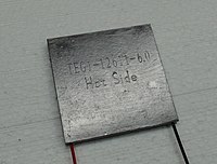
Photo from wikipedia
The development of eco‐friendly, ultralow‐power and easy‐to‐process electronics is facing dominant challenges in emerging off‐the‐grid applications, such as the Internet of Things (IoTs) and extreme environment explorations at the south/north… Click to show full abstract
The development of eco‐friendly, ultralow‐power and easy‐to‐process electronics is facing dominant challenges in emerging off‐the‐grid applications, such as the Internet of Things (IoTs) and extreme environment explorations at the south/north pole, in the deep sea, and in outer space. Eco‐friendly, biodegradable, lightweight, and flexible paper‐based electronics can provide many new possibilities for next‐generation devices and circuits. Here, enhancement‐mode (E‐mode, remaining off state at zero gate voltages) carbon nanotube (CNT) complementary metal‐oxide‐semiconductor (CMOS) thin‐film transistors (TFTs) are built on paper substrates through a printing‐based process. Benefitting from the CMOS circuit style and E‐mode transistors, the fabricated CMOS inverters exhibit high voltage gains (more than 11) and noise margins (up to 75% 1/2 VDD at VDD of 0.4 V), and rail‐to‐rail operation down to a VDD as low as 0.2 V and record low power dissipation as low as 0.0124 pW μm−1. Furthermore, the transistors and integrated circuits (ICs) show an excellent radiation tolerance of a total ionizing dose (TID) exceeding 2 Mrad with a high dose rate of 365 rad s−1. The record power consumption and outstanding radiation tolerance behavior achieved in paper‐based and easy‐to‐process CNT electronics are attractive for emerging energy‐saving and environmentally friendly ICs in harsh environment (such as outer‐space) applications.
Journal Title: Advanced Materials
Year Published: 2022
Link to full text (if available)
Share on Social Media: Sign Up to like & get
recommendations!