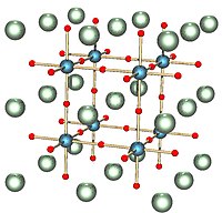
Photo from wikipedia
Engineering surface structure can precisely and effectively tune the optoelectronic properties of halide perovskites, but are incredibly challenging. Herein, the design and fabrication of uniform all‐inorganic CsPbBr3 cubic/tetrahedral single‐crystals are… Click to show full abstract
Engineering surface structure can precisely and effectively tune the optoelectronic properties of halide perovskites, but are incredibly challenging. Herein, the design and fabrication of uniform all‐inorganic CsPbBr3 cubic/tetrahedral single‐crystals are reported with precise control of the (100) and (111) surface anisotropy, respectively. By combining with theoretical calculations, it is demonstrated that the preferred (100) surface engineering of the CsPbBr3 single‐crystals enables a lowest surface bandgap energy (2.33 eV) and high‐rate carrier mobility up to 241 μm2 V‐1 s‐1, inherently boosting their light‐harvesting and carrier‐transport capability. Meanwhile, the polar (111) surface induces ≈0.16 eV upward surface‐band bending and ultrahigh surface defect density of 1.49 × 1015 cm‐3, which is beneficial for enhancing surface‐defects‐catalyzed reactions. The work highlights the anisotropic surface engineering for boosting perovskite optoelectronic devices and beyond.
Journal Title: Advanced Materials
Year Published: 2022
Link to full text (if available)
Share on Social Media: Sign Up to like & get
recommendations!