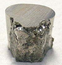
Photo from wikipedia
Porous germanium (PGe) nanostructures attract a lot of attention for various emerging applications due to their unique properties. Consequently, there is an increasing need for the development of low‐cost synthesis… Click to show full abstract
Porous germanium (PGe) nanostructures attract a lot of attention for various emerging applications due to their unique properties. Consequently, there is an increasing need for the development of low‐cost synthesis routes that are compatible with large‐scale production. Bipolar electrochemical etching (BEE) is a widely used solution for producing porous Ge layers. However, the lack of controllable production of large‐scale uniform PGe layers is the limiting factor for mainstream applications. Large‐scale homogeneous PGe layers formation is demonstrated by improving the BEE process. The PGe structures demonstrate excellent homogeneity in thickness and porosity, with a relative variation of below 2% across the 100 mm wafer. Furthermore, this process enables accurate tuning of the PGe's physical properties through variation of the etching parameters. PGe structures with porosity ranging from 40% to 80% and an adjustable thickness, while preserving low surface roughness are demonstrated, giving access to a large variety of PGe nanostructures for a wide range of applications. Ellipsometry and X‐ray reflectivity are employed to measure the porosity and thickness of PGe layers, providing fast and non‐destructive methods of characterization. These findings lay the groundwork for the large‐scale production of high‐quality PGe layers with on‐demand characteristics.
Journal Title: Advanced Materials Interfaces
Year Published: 2023
Link to full text (if available)
Share on Social Media: Sign Up to like & get
recommendations!