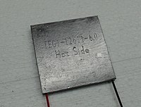
Photo from wikipedia
Recently, field‐effect transistors (FETs) based on two‐dimensional (2D) Bi2Te3 nanoplates have attracted much attention due to their great potential for fabricating high‐performance electronic devices. However, the gating property measurement of… Click to show full abstract
Recently, field‐effect transistors (FETs) based on two‐dimensional (2D) Bi2Te3 nanoplates have attracted much attention due to their great potential for fabricating high‐performance electronic devices. However, the gating property measurement of the Bi2Te3 nanoplate FETs exhibits hysteretic behavior in an ambient environment, which degrades not only their electrical properties, but also their device performance. This work presents a systematical study on the origins of this hysteresis effect in 2D Bi2Te3 FETs and explores effective approaches to minimize and eliminate this hysteresis effect. The hysteresis effect in 2D Bi2Te3 nanoplate FETs can be attributed to the charge trap states caused by the water molecules adsorbed on the nanoplate surface. To minimize and eliminate this hysteresis, poly(methyl methacrylate) layer is applied to passivate the 2D Bi2Te3 FETs, which leads to almost hysteresis‐free gating property and thus improves the carrier mobility and device performance. These results indicate that the surface/interface trap states of nanostructures can significantly influence their electrical properties and thus device performance, and as a result, surface passivation is required to minimize the influence of the surface/interface trap states and achieve high device performance.
Journal Title: Advanced Electronic Materials
Year Published: 2020
Link to full text (if available)
Share on Social Media: Sign Up to like & get
recommendations!