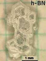
Photo from wikipedia
Atomically thin hexagonal boron nitride (h-BN) is gaining significant attention for many applications such as a dielectric layer or substrate for graphene-based devices. For these applications, synthesis of high-quality and… Click to show full abstract
Atomically thin hexagonal boron nitride (h-BN) is gaining significant attention for many applications such as a dielectric layer or substrate for graphene-based devices. For these applications, synthesis of high-quality and large-area h-BN layers with few defects is strongly desirable. In this work, the aligned growth of millimeter-size single-crystal h-BN domains on epitaxial Ni (111)/sapphire substrates by ion beam sputtering deposition is demonstrated. Under the optimized growth conditions, single-crystal h-BN domains up to 0.6 mm in edge length are obtained, the largest reported to date. The formation of large-size h-BN domains results mainly from the reduced Ni-grain boundaries and the improved crystallinity of Ni film. Furthermore, the h-BN domains show well-aligned orientation and excellent dielectric properties. In addition, the sapphire substrates can be repeatedly used with almost no limit. This work provides an effective approach for synthesizing large-scale high-quality h-BN layers for electronic applications.
Journal Title: Small
Year Published: 2017
Link to full text (if available)
Share on Social Media: Sign Up to like & get
recommendations!