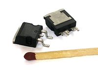
Photo from wikipedia
CMOS technology substrate crosstalk modeling and a respective analysis flow that captures the affected circuit performance is described. The proposed methodology can be seamlessly integrated into any industrial Analog/RF circuit… Click to show full abstract
CMOS technology substrate crosstalk modeling and a respective analysis flow that captures the affected circuit performance is described. The proposed methodology can be seamlessly integrated into any industrial Analog/RF circuit design flow, and be compatible within standard design environments. It provides accurate estimation of the substrate coupling effects and can estimate adequately all the mask design level isolation performance trends by adapting an advanced substrate modeling concept based on geometrical and process data. Different substrate model accuracy constraints can be invoked depending on the design phase and the simulation time needs. The provided accuracy is validated by correlating simulation results versus on wafer silicon measurements in a 28 nm CMOS set of ring oscillators with carrier frequency of 670 MHz. The mean error of the proposed method is 665 μV while the error sigma is 765 μV.
Journal Title: Analog Integrated Circuits and Signal Processing
Year Published: 2017
Link to full text (if available)
Share on Social Media: Sign Up to like & get
recommendations!