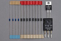
Photo from wikipedia
This work investigates a process-variation resilient electrostatically-doped ferroelectric Schottky-barrier tunnel FET (ED-FE-SB-TFET) based on negative capacitance (NC). The key attributes of ED-FE-SB-TFET are perovskite ferroelectric (FE) gate stack-induced NC behavior… Click to show full abstract
This work investigates a process-variation resilient electrostatically-doped ferroelectric Schottky-barrier tunnel FET (ED-FE-SB-TFET) based on negative capacitance (NC). The key attributes of ED-FE-SB-TFET are perovskite ferroelectric (FE) gate stack-induced NC behavior and electrostatic doping to induce pockets at both source/drain and channel interfaces. The positive feedback among the electric dipoles in FE material leads to intrinsic voltage amplification and enhanced gate controllability, thus it facilitates faster switching transitions. The proposed ED-FE-SB-TFET endeavors to create a substantial reduction in the ambipolar current ($$I_\mathrm{Amb}$$IAmb), steep sub-threshold slope, paramount boost in drive current, lower drain-induced barrier-lowering, and enhanced scalability. It also obviates the need for metallurgical doping, hence ion-implantation or dopant segregation techniques employed for planar SB-TFETs pocket-doping are no longer required, and it also modifies effective Schottky barrier height and Schottky tunneling barrier width significantly to enhance the device behavior. It offers a simplified fabrication process, and it is highly resilient towards process variations, doping control issues, and random dopant fluctuations. Moreover, there is a reduced thermal budget that facilitates its fabrication on single crystal silicon-on-glass substrate realized by wafer scale epitaxial transfer. Results reveal its potential as strong candidate for next generation, scaled and low power applications.
Journal Title: Journal of Computational Electronics
Year Published: 2017
Link to full text (if available)
Share on Social Media: Sign Up to like & get
recommendations!