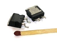
Photo from wikipedia
This manuscript describes an experimental comparative study of effects of the total ionizing dose (TID) on the main electrical parameters and figures of merit of Metal–Oxide–Semiconductor Field Effect Transistors (MOSFETs)… Click to show full abstract
This manuscript describes an experimental comparative study of effects of the total ionizing dose (TID) on the main electrical parameters and figures of merit of Metal–Oxide–Semiconductor Field Effect Transistors (MOSFETs) implemented with two different layout styles, i.e., the hexagonal gate shape (diamond MOSFET, DM) and its corresponding rectangular counterparts (Conventional MOSFET, CM), which they were irradiated with a low dose rate with gamma-rays (60Co-source), considering that both present the same gate areas (AG), channel widths (W), aspect ratios (W/L), and concerning two different bias conditions (OFF and ON states) during the irradiation procedure. The main results of this work show that, besides the diamond MOSFETs present a better electrical performance than those found in their Conventional MOSFETs counterparts, they are also capable of boosting their ionizing radiation tolerances (smaller variation of the threshold voltage, subthreshold slope and minimize IDS leakage, etc.). Furthermore, it was observed that the hexagonal gate shape with a α angle equal to 90° tends to be the best gate geometry for MOSFETs because it is capable of enhancing the TID tolerance, intrinsically, in relation to the CM counterparts, regarding gamma-rays source used in this study. Therefore, the diamond layout style with α angle of 90° can be considered an alternative Hardness-By-Design layout technique which is able to manufacture planar MOSFETs low-cost, high electrical performance, and high ionizing tolerance to be applied in the space, medical, and nuclear CMOS ICs applications.
Journal Title: Journal of Materials Science: Materials in Electronics
Year Published: 2019
Link to full text (if available)
Share on Social Media: Sign Up to like & get
recommendations!