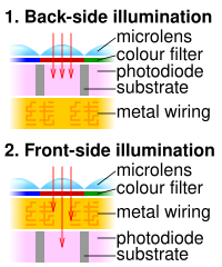
Photo from wikipedia
In this paper, the back-illuminated In0.09Ga0.91N p-i-n ultraviolet photodetectors have been fabricated and simulated. The responsivity characteristic was shown experimentally and theoretically. The peak responsivity of photodetector was improved from… Click to show full abstract
In this paper, the back-illuminated In0.09Ga0.91N p-i-n ultraviolet photodetectors have been fabricated and simulated. The responsivity characteristic was shown experimentally and theoretically. The peak responsivity of photodetector was improved from 0.06 A/W at 394 nm to 0.19 A/W at 402 nm since the growth of a 30 nm i-GaN layer between i-InGaN layer and n-GaN layer. The photodetector models and characteristics were numerical simulated and optimized by Silvaco TCAD semiconductor simulation software. The simulation results revealed that the responsivity has great relationship with the Shockley-Read-Hall recombination lifetime, intrinsic layer thickness and extinction coefficient k. In addition, the simulation results were in good agreement with the experimental results when the SRH recombination lifetime about 0.01-0.1 ns and the In composition x introduced a 0.05 increment of In0.09Ga0.91N layer.
Journal Title: Optical and Quantum Electronics
Year Published: 2017
Link to full text (if available)
Share on Social Media: Sign Up to like & get
recommendations!