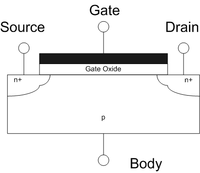
Photo from wikipedia
This paper presents an efficient method to improve the heating effects in Nanoscale SOI MOSFET with the Vertical Gaussian Doping Profile in Drain and Source regions (D-S-G-SOI). Three different structures… Click to show full abstract
This paper presents an efficient method to improve the heating effects in Nanoscale SOI MOSFET with the Vertical Gaussian Doping Profile in Drain and Source regions (D-S-G-SOI). Three different structures are investigated: uniform drain (C-SOI), Gaussian drain doping profile (D-G-SOI) SOI MOSFET, and drain-source region with Gaussian doping profile (D-S-G-SOI) and results are compared. Gaussian doping function parameters like standard variation (σ) are used in our study. The proposed structure has been compared with other structures in terms of the lattice temperature, sub-threshold slope, electric potential, electric field, DIBL, leakage current, and floating body (Kink effect). Our results show the excellent electrical and thermal performance of the proposed structure taken account of as a proper substitution for the conventional device.
Journal Title: Silicon
Year Published: 2020
Link to full text (if available)
Share on Social Media: Sign Up to like & get
recommendations!