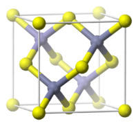
Photo from wikipedia
Abstract Nanocrystalline PbTe thin films were deposited on a glass substrate by thermal evaporation technique with two thicknesses namely, 45 and 250 nm. The structural studies revealed that the films have… Click to show full abstract
Abstract Nanocrystalline PbTe thin films were deposited on a glass substrate by thermal evaporation technique with two thicknesses namely, 45 and 250 nm. The structural studies revealed that the films have nanocrystalline cubic structure and the particle size was found to be 11 and 20.7 nm, for low and high thicknesses respectively. The FE-SEM study shows that the surface grains increase for higher thickness film. This indicates that samples lying under the strong regime of confinement for PbTe thin films. The optical properties confirm the occurrence of confinement process as the optical band gap are 1.67 and 0.9 eV for 45 and 250 nm films, respectively. The dielectric results indicated that the conductivity increases by about two orders of magnitude with increasing the thickness from 45 to 250 nm. Moreover, the permittivity shows a higher dispersion step at lower frequencies in both samples due to the hopping conduction mechanism in addition to the interfacial polarization in such heterogeneous structures. Another small dispersion step is noticed in case of the lower thickness. It is attributed to the polarization of the accumulated charge carriers near the grain boundaries interfaces. No indication of any electrode phenomena in both samples is shown here.
Journal Title: Current Applied Physics
Year Published: 2019
Link to full text (if available)
Share on Social Media: Sign Up to like & get
recommendations!