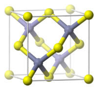
Photo from wikipedia
Abstract Many physical characteristics of semiconducting materials can be finely controlled through template-based nanostructure growth, leading to tuning their properties as well. Reproducible through-hole growth of customised semiconducting nanotubes on… Click to show full abstract
Abstract Many physical characteristics of semiconducting materials can be finely controlled through template-based nanostructure growth, leading to tuning their properties as well. Reproducible through-hole growth of customised semiconducting nanotubes on Al2O3 (AAO) template is challenging; and therefore, their production methods are of utmost importance. An efficient approach is demonstrated here to remove the sensitive barrier layer from micron thick AAO template keeping base aluminium intact, which serves as an ohmic contact. To prove the effectiveness of this approach, high aspect ratio Cadmium telluride nanotubes (CdTe NTs) having controllable diameter were synthesized using DC electrodeposition. FE-SEM and TEM micrographs illustrate the growth of through-hole nanotubes at each stage of barrier layer etching in AAO template. CdTe nanotubes with an average diameter of 80 nm, grown under various electrolyte baths, have been studied using XRD and Raman spectroscopy. Raman study was done at 77 K to check the confinement effect on multiphonon Raman scattering of LO mode in CdTe NTs. As grown nanotubes show strong luminescence in the visible region with enhanced optical bandgap, and high purity demonstrated by X-ray photoelectron spectroscopy. Excellent specific capacitance of 332 F g-1 at scan rate 100 mV s-1 was found for CdTe-NTs in 6 mol L-1 KOH electrolyte. Efficient photoluminescence (PL) emission and the increase in specific capacitance proved to be worthy for its applications in photovoltaics and energy-storage devices.
Journal Title: Journal of Alloys and Compounds
Year Published: 2019
Link to full text (if available)
Share on Social Media: Sign Up to like & get
recommendations!