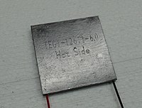
Photo from wikipedia
Abstract P- and n-doped bismuth telluride (Bi2Te3) polycrystalline nanostructures were prepared on structured PECVD-oxide-layers using magnetron sputtering and a lithography independent deposition and back-etching step. The resulting polycrystalline spacer-structures have… Click to show full abstract
Abstract P- and n-doped bismuth telluride (Bi2Te3) polycrystalline nanostructures were prepared on structured PECVD-oxide-layers using magnetron sputtering and a lithography independent deposition and back-etching step. The resulting polycrystalline spacer-structures have adjustable dimensions with heights of 350 to 450 nm, a widths of 200 to 220 nm and a fix length of 1240 μm and 4020 μm. This paper presents the production of Bi2Te3 structures and how annealing affects the electrical conductivity in order to improve their potential in thermoelectric applications. In addition to temperature variation and multiple annealing the influence of different atmospheres during the annealing step has been investigated. It is shown that the electrical conductivity of the p-doped material increases by a factor of 1.8, while it decreases for the n-doped material.
Journal Title: Microelectronic Engineering
Year Published: 2019
Link to full text (if available)
Share on Social Media: Sign Up to like & get
recommendations!