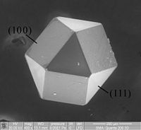
Photo from wikipedia
Abstract In the X-ray photoelectron spectroscopy experiment, we observed that the valence band spectrum of the n-GaN (0001) surface appeared a bump near 1.9 eV after Ar etching and the N/Ga… Click to show full abstract
Abstract In the X-ray photoelectron spectroscopy experiment, we observed that the valence band spectrum of the n-GaN (0001) surface appeared a bump near 1.9 eV after Ar etching and the N/Ga ratio became smaller, while the bump disappeared upon exposure to air. In order to analyze this phenomenon theoretically, we mainly study the electronic structure and optical properties of n-GaN (0001) surface with N vacancy and filled with O atom based on the first principles of density functional theory. The results suggest that the n-GaN (0001) surface exhibits semi-metallic property. The introduction of N vacancy reduces the n-type conductivity, whereas the filling of O atom enhances conductivity. The density of state near −1.9eV shows a good agreement between the clean n-type surface and the O-atom-filled surface, while the N vacancy surface has a higher density of states, which is similar to the experimentally observed phenomenon. It is also found that the existence of N vacancy reduces the photoemission properties of the n-GaN (0001) surface and the filling of O atom alleviates the defect caused by vacancy. This study shows that N vacancy increases the doping difficulty of n-type GaN films, however, the filling of O atom may compensate for the diminished photoelectric properties induced by N vacancy and be conducive to prepare high-performance optoelectronic devices with the contact of n-GaN and metal.
Journal Title: Superlattices and Microstructures
Year Published: 2018
Link to full text (if available)
Share on Social Media: Sign Up to like & get
recommendations!