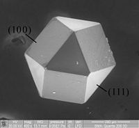
Photo from wikipedia
Abstract Thickness-controlled separation of a thin layer of single-crystalline semiconductors from its bulk substrate has been developed for the co-integration of compound semiconductors with silicon-based integrated circuit chips and the… Click to show full abstract
Abstract Thickness-controlled separation of a thin layer of single-crystalline semiconductors from its bulk substrate has been developed for the co-integration of compound semiconductors with silicon-based integrated circuit chips and the fabrication of high-performance flexible devices. Recently, a controlled spalling technique that can mechanically separate single-crystalline semiconductor layers has been actively demonstrated because of the process simplicity and the less limitation on the use of materials. Here, we developed an analytic model that can precisely estimate the spalling depth. In this model, the spalling depth was calculated from the thermodynamic equilibrium condition in which total strain energy accumulated in a separated layer is balanced with the crystal binding energy. We experimentally investigated the dependence of the spalling depth on the stressor layer thickness and stress, and we compared the empirical results with the proposed analytic model. We also verified that the crack initiation angle of the spalling process is determined by the binding energy contrast in the main crystal orientations in the semiconductor.
Journal Title: Solid-state Electronics
Year Published: 2020
Link to full text (if available)
Share on Social Media: Sign Up to like & get
recommendations!