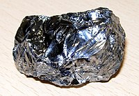
Photo from wikipedia
Silicon (Si) zigzag nanowires (NWs) have a great potential in many applications because of its high surface/volume ratio. However, fabricating Si zigzag NWs has been challenging. In this work, a… Click to show full abstract
Silicon (Si) zigzag nanowires (NWs) have a great potential in many applications because of its high surface/volume ratio. However, fabricating Si zigzag NWs has been challenging. In this work, a diffusion-controlled metal-assisted chemical etching method is developed to fabricate Si zigzag NWs. By tailoring the composition of etchant to change its diffusivity, etching direction, and etching time, various zigzag NWs can be easily fabricated. In addition, it is also found that a critical length of NW (>1 μm) is needed to form zigzag nanowires. Also, the amplitude of zigzag increases as the location approaches the center of the substrate and the length of zigzag nanowire increases. It is also demonstrated that such zigzag NWs can help the silicon substrate for self-cleaning and antireflection. This method may provide a feasible and economical way to fabricate zigzag NWs and novel structures for broad applications.
Journal Title: Nano letters
Year Published: 2017
Link to full text (if available)
Share on Social Media: Sign Up to like & get
recommendations!