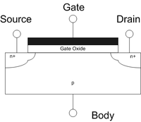
Photo from wikipedia
Here, we demonstrate side-gated in-plane structure of solution-processed amorphous oxide semiconductor (AOS) ionotronic devices and logic circuits enabled by ion-gel gate dielectrics with monolithically integrated nanoscale passivation architecture. The large… Click to show full abstract
Here, we demonstrate side-gated in-plane structure of solution-processed amorphous oxide semiconductor (AOS) ionotronic devices and logic circuits enabled by ion-gel gate dielectrics with monolithically integrated nanoscale passivation architecture. The large capacitance of electric double layer (EDL) in the ion-gel allows a device structure to be a side gate geometry, forming an in-plane structured amorphous In-Ga-Zn-O (a-IGZO) ionotronic transistor which can be translated into a simplified logic gate configuration with a low operation voltage. Particularly, the monolithic passivation of the coplanar electrodes offers advantages over conventional inhomogeneous passivation, mitigating unintentional parasitic leakage current through ion-gel dielectric layer. More importantly, the monolithically integrated passivation over electrodes was readily obtained with CMOS compatible photochemical process by employing a controlled ultraviolet light manipulation under ozone ambient, which introduced not only much enhanced electrical characteristics but also a scalable device architecture. We investigated various electrical behaviors of the side gated a-IGZO ionotronic transistor based on EDL, which is called electric double layer transistor (EDLT), and logic circuits enabled by photochemically realized monolithic aluminum oxide (AlOX) passivation comparing to the native or polymerized passivation layer, which reveals that the photo-assisted AlOX secures high performance a-IGZO EDLTs with a low off current (< 5.23 × 10⁻⁸ A), high on/off ratio (>1.87 × 10⁵), and exceptional high carrier mobility (>14.5 cm2 V-1s-1). Owing to the significantly improved electrical characteristics, an inverter circuit was successfully achieved with broad operation voltages from ultra-low VDD of 1 mV to 1.5 V, showing a fully logical voltage transfer characteristic with gain of more than 4 V V-1.
Journal Title: ACS applied materials & interfaces
Year Published: 2020
Link to full text (if available)
Share on Social Media: Sign Up to like & get
recommendations!