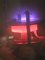
Photo from wikipedia
A laser-induced doping method was employed to incorporate phosphorus into an insulating monocrystalline diamond at ambient temperature and pressure conditions. Pulsed laser beams with nanosecond duration (20 ns) were irradiated… Click to show full abstract
A laser-induced doping method was employed to incorporate phosphorus into an insulating monocrystalline diamond at ambient temperature and pressure conditions. Pulsed laser beams with nanosecond duration (20 ns) were irradiated on the diamond substrate immersed in a phosphoric acid liquid, in turns, and a thin conductive layer was formed on its surface. Phosphorus incorporation in the depth range of 40-50 nm below the irradiated surface was confirmed by secondary ion mass spectroscopy (SIMS). Electrically, the irradiated areas exhibited ohmic contacts even with tungsten prober heads at room temperature, where the electrical resistivity of irradiated areas was greatly decreased compared to the original surface. The temperature dependence of the electrical conductivity implies that the surface layer is semiconducting with activation energies ranging between 0.2 eV and 54 meV depending on irradiation conditions. Since after laser treatment no carbon or graphitic phases other than diamond is found (the D and G Raman peaks are barely observed), the incorporation of phosphorus is the main origin of the enhanced conductivity. It was demonstrated that the proposed technique is applicable to diamond as a new ex situ doping method for introducing impurities into a solid in a precise and well-controlled manner, especially with electronic technology targeting of smaller devices and shallower junctions.
Journal Title: ACS applied materials & interfaces
Year Published: 2020
Link to full text (if available)
Share on Social Media: Sign Up to like & get
recommendations!