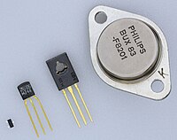
Photo from wikipedia
We present the device properties of a nickel (Ni)–gallium oxide (Ga2O3) Schottky junction with an interfacial hexagonal boron nitride (hBN) layer. A vertical Schottky junction with the configuration Ni/hBN/Ga2O3/In was… Click to show full abstract
We present the device properties of a nickel (Ni)–gallium oxide (Ga2O3) Schottky junction with an interfacial hexagonal boron nitride (hBN) layer. A vertical Schottky junction with the configuration Ni/hBN/Ga2O3/In was created using a chemical vapor-deposited hBN film on a Ga2O3 substrate. The current–voltage characteristics of the Schottky junction were investigated with and without the hBN interfacial layer. We observed that the turn-on voltage for the forward current of the Schottky junction was significantly enhanced with the hBN interfacial film. Furthermore, the Schottky junction was analyzed under the illumination of deep ultraviolet light (254 nm), obtaining a photoresponsivity of 95.11 mA/W under an applied bias voltage (−7.2 V). The hBN interfacial layer for the Ga2O3-based Schottky junction can serve as a barrier layer to control the turn-on voltage and optimize the device properties for deep-UV photosensor applications. Furthermore, the demonstrated vertical heterojunction with an hBN layer has the potential to be significant for temperature management at the junction interface to develop reliable Ga2O3-based Schottky junction devices.
Journal Title: ACS Omega
Year Published: 2022
Link to full text (if available)
Share on Social Media: Sign Up to like & get
recommendations!