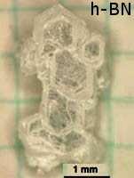
Photo from wikipedia
Contactless electroreflectance studies coupled with numerical calculations are performed on in-situ SiNx capped N-polar III-nitride high electron mobility transistor (HEMT) structures with a scaled channel thickness in order to analyse… Click to show full abstract
Contactless electroreflectance studies coupled with numerical calculations are performed on in-situ SiNx capped N-polar III-nitride high electron mobility transistor (HEMT) structures with a scaled channel thickness in order to analyse the built-in electric field in the GaN channel layer. The experimentally obtained field values are compared with the calculated field versus channel thickness curves. Furthermore, the experimental and theoretical sheet carrier densities, ns, are evaluated. While a gradual decrease in carrier concentration with decreasing channel thickness is expected for N-polar structures, experimentally a sudden drop in the ns values is observed for samples with very thin channels. The additional loss in charge was associated with a change in the SiNx/AlGaN interface Fermi level at very thin channel thicknesses.
Journal Title: Scientific Reports
Year Published: 2020
Link to full text (if available)
Share on Social Media: Sign Up to like & get
recommendations!