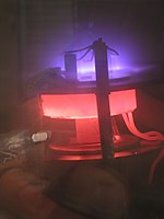
Photo from wikipedia
Gallium nitride (GaN) was epitaxially grown on nitrogen doped single layer graphene (N-SLG) substrates using chemical vapour deposition (CVD) technique. The results obtained using x-ray diffractometer (XRD) revealed the hexagonal… Click to show full abstract
Gallium nitride (GaN) was epitaxially grown on nitrogen doped single layer graphene (N-SLG) substrates using chemical vapour deposition (CVD) technique. The results obtained using x-ray diffractometer (XRD) revealed the hexagonal crystal structure of GaN. Photoluminescence (PL) spectroscopy, energy dispersive x-ray (EDX) spectroscopy and x-ray photoelectron (XPS) spectroscopy revealed traces of oxygen, carbon and nitrogen occurring either as contamination or as an effect of doping during the GaN growth process. In addition, PL revealed a weak yellow luminescence peak in all the samples due to the presence of N-SLG. From the obtained results it was evident that, presence of N-SLG underneath GaN helped in improving the material properties. It was seen from the current–voltage (I–V) response that the barrier height estimated is in good agreement with the Schottky–Mott model, while the ideality factor is close to unity, emphasizing that there are no surface and interface related inhomogeneity in the samples. The photodetector fabricated with this material exhibit high device performances in terms of carrier mobility, sensitivity, responsivity and detectivity. The hall measurement values clearly portray that, the GaN thus grown possess high electron contents which was beneficial in attaining extraordinary device performance.
Journal Title: Scientific Reports
Year Published: 2020
Link to full text (if available)
Share on Social Media: Sign Up to like & get
recommendations!