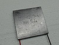
Photo from wikipedia
Nanowire geometry allows semiconductor heterostructures to be obtained that are not achievable in planar systems, as in, for example, axial superlattices made of large lattice mismatched materials. This provides a… Click to show full abstract
Nanowire geometry allows semiconductor heterostructures to be obtained that are not achievable in planar systems, as in, for example, axial superlattices made of large lattice mismatched materials. This provides a great opportunity to explore new optical transitions and vibrational properties resulting from the superstructure. Moreover, superlattice nanowires are expected to show improved thermoelectric properties, owing to the dominant role of surfaces and interfaces that can scatter phonons more effectively, reducing the lattice thermal conductivity. Here, we show the growth of long (up to 100 repetitions) GaAs/GaP superlattice nanowires with different periodicities, uniform layer thicknesses, and sharp interfaces, realized by means of Au-assisted chemical beam epitaxy. By optimizing the growth conditions, we obtained great control of the nanowire diameter, growth rate, and superlattice periodicity, offering a valuable degree of freedom for engineering photonic and phononic properties at the nanoscale. As a proof of concept, we analyzed a single type of superlattice nanowire with a well-defined periodicity and we observed room temperature optical emission and new phonon modes. Our results prove that high-quality GaAs/GaP superlattice nanowires have great potential for phononic and optoelectronic studies and applications.
Journal Title: Nanoscale
Year Published: 2022
Link to full text (if available)
Share on Social Media: Sign Up to like & get
recommendations!