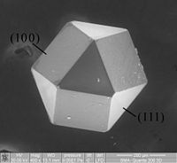
Photo from wikipedia
The exfoliation and identification of the two-dimensional (2D) single atomic layer of carbon have opened the opportunity to explore graphene and related 2D materials due to their unique properties. 2D… Click to show full abstract
The exfoliation and identification of the two-dimensional (2D) single atomic layer of carbon have opened the opportunity to explore graphene and related 2D materials due to their unique properties. 2D materials are regarded as one of the most exciting solutions for next generation electronics and optoelectronics in the technological evolution of semiconductor technology. In this review, we focus on the core concept of “structure-property relationships” to explain the state-of-the-art of 2D materials and summarize the unique electrical and light-matter interaction properties in 2D materials. Based on this, we discuss and analyze the structural properties of 2D materials, such as defects and dopants, the number of layers, composition, phase, strain, and other structural characteristics, which could significantly alter the properties of 2D materials and hence affect the performance of semiconductor devices. In particular, the building blocks principles and potential electronic and optoelectronic applications...
Journal Title: Applied physics reviews
Year Published: 2017
Link to full text (if available)
Share on Social Media: Sign Up to like & get
recommendations!