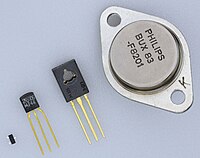
Photo from wikipedia
We proposed a two-terminal-electrode vertical thyristor and investigated its suitability as a cross-point memory cell without a selector from the viewpoints of p+- and n+-base region width and a vertically… Click to show full abstract
We proposed a two-terminal-electrode vertical thyristor and investigated its suitability as a cross-point memory cell without a selector from the viewpoints of p+- and n+-base region width and a vertically stacked doped-epitaxial-Si layer structure such as p++-emitter/n+-base/p+-base/n++-emitter or n++-emitter/p+-base/n+-base/p++-emitter. The proper p+- and n+-base-region width (i.e., 160 nm) and p++-emitter/n+-base/p+-base/n++-emitter layer structure could enable the development of a cross-point memory cell using the half bias concept by preventing misfit dislocations at the junctions between the n++-emitter and p+-base or n+-base and p++-emitter. It was also found that generation of the misfit dislocations originating from B or P atom segregation at junctions during doped-Si epitaxial-layer growth enhanced the strain at the junctions. The misfit dislocations at the junctions were produced when the strain at the junctions was greater than ∼4 × 10⁻⁴.We proposed a two-terminal-electrode vertical thyristor and investigated its suitability as a cross-point memory cell without a selector from the viewpoints of p+- and n+-base region width and a vertically stacked doped-epitaxial-Si layer structure such as p++-emitter/n+-base/p+-base/n++-emitter or n++-emitter/p+-base/n+-base/p++-emitter. The proper p+- and n+-base-region width (i.e., 160 nm) and p++-emitter/n+-base/p+-base/n++-emitter layer structure could enable the development of a cross-point memory cell using the half bias concept by preventing misfit dislocations at the junctions between the n++-emitter and p+-base or n+-base and p++-emitter. It was also found that generation of the misfit dislocations originating from B or P atom segregation at junctions during doped-Si epitaxial-layer growth enhanced the strain at the junctions. The misfit dislocations at the junctions were produced when the strain at the junctions was greater than ∼4 × 10⁻⁴.
Journal Title: Applied Physics Letters
Year Published: 2018
Link to full text (if available)
Share on Social Media: Sign Up to like & get
recommendations!