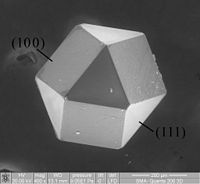
Photo from wikipedia
The growth of GaN nanocrystals in an amorphous SiO2 matrix by sequential Ga and N implantation and rapid thermal annealing is reported. The effect of the implantation and annealing conditions… Click to show full abstract
The growth of GaN nanocrystals in an amorphous SiO2 matrix by sequential Ga and N implantation and rapid thermal annealing is reported. The effect of the implantation and annealing conditions on the distribution of the implanted ions, as well as the size, static disorder, and stability of the grown GaN nanocrystals, is studied by means of transmission electron microscopy, Rutherford backscattering spectrometry, Raman scattering, and extended X-ray absorption fine structure spectroscopies. It is found that the optimum temperature range for the post-implantation annealing of the nanocrystals, with a size that ranges from about 3 to 12 nm, is 1000–1100 °C. Higher temperatures result in the dissociation of the nanocrystals and out-diffusion of N and Ga, whereas lower temperatures are insufficient for the growth of GaN nanocrystals. Annealing for 30–90 s is optimum in order to avoid considerable loss of N and Ga. However, upon annealing at higher temperatures within the optimum range, up to 1100 °C, or for longer times, up to 120 s, larger GaN nanocrystals are grown and/or lower static disorder is observed.The growth of GaN nanocrystals in an amorphous SiO2 matrix by sequential Ga and N implantation and rapid thermal annealing is reported. The effect of the implantation and annealing conditions on the distribution of the implanted ions, as well as the size, static disorder, and stability of the grown GaN nanocrystals, is studied by means of transmission electron microscopy, Rutherford backscattering spectrometry, Raman scattering, and extended X-ray absorption fine structure spectroscopies. It is found that the optimum temperature range for the post-implantation annealing of the nanocrystals, with a size that ranges from about 3 to 12 nm, is 1000–1100 °C. Higher temperatures result in the dissociation of the nanocrystals and out-diffusion of N and Ga, whereas lower temperatures are insufficient for the growth of GaN nanocrystals. Annealing for 30–90 s is optimum in order to avoid considerable loss of N and Ga. However, upon annealing at higher temperatures within the optimum range, up to 1100 °C, or for lon...
Journal Title: Journal of Applied Physics
Year Published: 2020
Link to full text (if available)
Share on Social Media: Sign Up to like & get
recommendations!