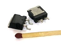
Photo from wikipedia
CdS nanowires and film Schottky diodes are fabricated and diode properties are compared. Effect of SnO2 on CdS film diode properties is investigated. CdS film/Au on 100 nm SnO2 substrate… Click to show full abstract
CdS nanowires and film Schottky diodes are fabricated and diode properties are compared. Effect of SnO2 on CdS film diode properties is investigated. CdS film/Au on 100 nm SnO2 substrate demonstrates like-resistor characteristics and increase in SnO2 thickness corrects resistor behavior, however the effective reverse saturation current density J o is significantly high and shunt resistance are considerably low, implying that SnO2 slightly prevents impurities migration from CdS films into ITO but cause additional issues. Thickness of CdS film on diode properties is further investigated and increasing CdS film thickness improved J o by one order of magnitude, however shunt resistance is obviously low, suggesting intrinsic issues in CdS film. 100 nm CdS nanowire/Au diodes reduce J o by three orders of magnitude in the dark and two orders of magnitude in the light respectively and their shunt resistance is significantly enhanced by 70 times when comparing with those of the CdS film diodes. The wide difference can be attributed to the fact that CdS nanowires overcome intrinsic issues in CdS film and thus demonstrate significantly well- defined diode behavior. Simulation found that CdS nanowire diodes have low compensating acceptor type traps and interface state density of 5.0 × 109 cm−2, indicating that interface recombination is not a dominated current transport mechanism in the nanowire diodes. CdS film diodes are simulated with acceptor traps and interface state density increased by two order of magnitude and shunt resistance reduced by one order of magnitude, indicating that high density of interface states and shunt paths occur in the CdS film diodes.
Journal Title: Nanotechnology
Year Published: 2022
Link to full text (if available)
Share on Social Media: Sign Up to like & get
recommendations!