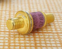
Photo from wikipedia
In this paper, a submillimeter-wave Schottky diode is designed and simulated. Effect of Schottky layer thickness on cut-off frequency is studied. A novel microfabrication process is proposed and implemented. The… Click to show full abstract
In this paper, a submillimeter-wave Schottky diode is designed and simulated. Effect of Schottky layer thickness on cut-off frequency is studied. A novel microfabrication process is proposed and implemented. The presented microfabrication process avoids electron-beam (e-beam) lithography which reduces the cost. Also, this process provides more flexibility in selection of design parameters and allows significant reduction in the device parasitic capacitance. A key feature of the process is that the Schottky contact, the air-bridges, and the transmission lines, are fabricated in a single lift-off step. This process relies on a planarization method that is suitable for trenches of 1–10 μm deep and is tolerant to end-point variations. The fabricated diode is measured and results are compared with simulations. A very good agreement between simulation and measurement results are observed.
Journal Title: Semiconductor Science and Technology
Year Published: 2017
Link to full text (if available)
Share on Social Media: Sign Up to like & get
recommendations!