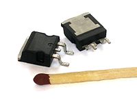
Photo from wikipedia
In this research, based on I–V and C–V measurement at different temperatures, the interface defect density in the device with the Si/SiGe channel was discussed. In addition, negative bias temperature… Click to show full abstract
In this research, based on I–V and C–V measurement at different temperatures, the interface defect density in the device with the Si/SiGe channel was discussed. In addition, negative bias temperature instability (NBTI) is also studied. In previous research, most of the flat-band voltage (V FB) shifts during NBTI stress was attributed to hole injection. In this article, however, the release of atomic hydrogen from the Si–H bonds at the SiO2/Si interface and at the SiGe interface produces a fixed oxide charge, which causes V FB shifts which vary with material.
Journal Title: Semiconductor Science and Technology
Year Published: 2021
Link to full text (if available)
Share on Social Media: Sign Up to like & get
recommendations!