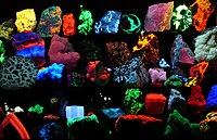
Photo from wikipedia
We have studied the surface structure of single-crystal, wide-gap semiconductor $\ensuremath{\beta}\text{\ensuremath{-}}{\mathrm{Ga}}_{2}{\mathrm{O}}_{3}(010)$ using x-ray photoelectron diffraction (XPD), low-energy electron diffraction (LEED), and x-ray photoelectron spectroscopy (XPS). The XPS measurements show typical… Click to show full abstract
We have studied the surface structure of single-crystal, wide-gap semiconductor $\ensuremath{\beta}\text{\ensuremath{-}}{\mathrm{Ga}}_{2}{\mathrm{O}}_{3}(010)$ using x-ray photoelectron diffraction (XPD), low-energy electron diffraction (LEED), and x-ray photoelectron spectroscopy (XPS). The XPS measurements show typical spectra for stoichiometric ${\mathrm{Ga}}_{2}{\mathrm{O}}_{3}(010)$. Annealing in vacuum produced a sharp ($1\ifmmode\times\else\texttimes\fi{}1$) LEED pattern, characteristic of the monoclinic structure. The XPD angular anisotropies were collected for the Ga $2{p}_{3/2}$ and O $1s$ core levels. Surface interlayer relaxation up to 8% of the bulk interplanar distance and 0.11--0.14 $\AA{}$ rumpling are observed at the $\ensuremath{\beta}\text{\ensuremath{-}}{\mathrm{Ga}}_{2}{\mathrm{O}}_{3}(010)$ surface. At the surface, the oxygen atoms shift toward the vacuum with respect to the gallium atoms. The rumpling decreases to zero and and the interplanar distance reaches the bulk value of 1.52 $\AA{}$ by the sixth atomic layer. The surface structure agrees with that predicted by first-principles density functional theory calculations which, in addition, suggest a significant band gap narrowing of $\ensuremath{\approx}1$ eV in the surface layer, due to surface states spatially localized on surface oxygen atoms of ${\mathrm{O}}_{\mathrm{II}}$ type.
Journal Title: Physical Review B
Year Published: 2020
Link to full text (if available)
Share on Social Media: Sign Up to like & get
recommendations!