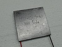
Photo from wikipedia
The recent renaissance in machine learning is requesting computing power at an ever-increasing rate. In order to meet this demand, tensor processing units (TPU) are becoming popular because they hold… Click to show full abstract
The recent renaissance in machine learning is requesting computing power at an ever-increasing rate. In order to meet this demand, tensor processing units (TPU) are becoming popular because they hold the promise to be more efficient in terms of power usage as well as throughput compared to GPUs. This is achieved by integrating a huge number of matrix-multiply units (MMU) to perform a massive amount of parallel multiply-accumulate operations. However, this causes excessive localized hot-spots. Elevated on-chip temperatures jeopardize reliability and significantly reduce the lifetime of semiconductor devices by accelerating aging defects. Therefore, it is vital to obtain accurate thermal maps of the TPU die at the design time to ensure reliability requirements during the run-time. Due to the high power density, traditional forced air convection cooling is often insufficient. Hence, liquid cooling may seem promising, but it requires substantial maintenance effort. To overcome this challenge, novel cooling concepts need to be explored. Recent advances in thermoelectric coolers (TEC), more specifically ultra thin-film superlattice thermoelectric (TE) devices, have opened new doors to combat this obstacle. To this end, finite-element (FEM) simulations enable designers to find tradeoffs between temperature and cooling cost. However, such multi-physics simulations are extremely time-consuming, which prevents designers from exploring the available design-space. In this work, we demonstrate a neural network (NN) model that captures the effects of a superlattice TEC device mounted on top of a TPU die. The additional required cooling cost is also estimated. The commercial multi-physics tool ANSYS® is employed in order to obtain high resolution data towards training the NN model. Our NN model allows to speed up the design-space exploration considerably, reducing the time required to generate a single thermal map from, on average, 45 min in ANSYS. to merely 70 ms with an average prediction error of 0.26°C. Our model covers a wide range of design parameters, such as convection film coefficient, power density and superlattice TEC cooling intensity.
Journal Title: IEEE Access
Year Published: 2022
Link to full text (if available)
Share on Social Media: Sign Up to like & get
recommendations!