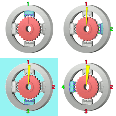
Photo from wikipedia
A power and area efficient two-step hybrid voltage–time ADC achieves a 4-GS/s conversion speed and 39.9-dB SNDR in 28-nm CMOS. Two pipelined time-based converters (TBCs) with a thermometer capacitive DAC… Click to show full abstract
A power and area efficient two-step hybrid voltage–time ADC achieves a 4-GS/s conversion speed and 39.9-dB SNDR in 28-nm CMOS. Two pipelined time-based converters (TBCs) with a thermometer capacitive DAC (CDAC) in the ADC lead to a high-speed and low-power operation. The pipelined architecture splits the full ADC resolution, thus relaxing the TBC complexity. The TBC consists of a voltage-domain comparator, a current-source-based voltage-to-time converter (VTC), and a ring oscillator (RO)-based time-to-digital converter (TDC) with feedforward and 2
Journal Title: IEEE Journal of Solid-State Circuits
Year Published: 2020
Link to full text (if available)
Share on Social Media: Sign Up to like & get
recommendations!