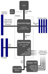
Photo from wikipedia
We present a two-stage cascaded clock multiplier with roughly constant energy consumption across 2.5-5.0GHz frequency range. The proposed clock multiplier consists of a reconfigurable delay-locked loop and edge combiner in… Click to show full abstract
We present a two-stage cascaded clock multiplier with roughly constant energy consumption across 2.5-5.0GHz frequency range. The proposed clock multiplier consists of a reconfigurable delay-locked loop and edge combiner in the first stage while generating a 156.25-312.5MHz clock from 39.0625MHz reference clock frequency. An injection-locked clock multiplier with a frequency tracking loop in the second stage implements a 2.5-5.0 GHz output clock. The clock generation architecture is optimized for the clock multiplication ratio in the two stages and overall power consumption. Designed in TSMC 65nm CMOS process and characterized with post-layout simulations, the first-stage clock multiplier achieves an integrated jitter 1.396-0.607ps
Journal Title: IEEE Transactions on Circuits and Systems II: Express Briefs
Year Published: 2022
Link to full text (if available)
Share on Social Media: Sign Up to like & get
recommendations!