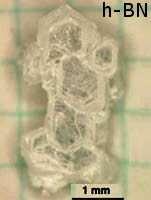
Photo from wikipedia
Black phosphorus (BP) has been proposed as the channel material in the next generation ultrascaled CMOS devices. In order to gain insight into the current characteristics in 2-D layered materials,… Click to show full abstract
Black phosphorus (BP) has been proposed as the channel material in the next generation ultrascaled CMOS devices. In order to gain insight into the current characteristics in 2-D layered materials, the current distribution of a few-layer BP Schottky barrier FET is investigated via state-of-the-art quantum device simulations. Approximately 40% of the total current was found to be concentrated in the top layer when the device was switched on, with the remaining current distributed among the other layers. In comparison, ~80% of the current concentrated below the surface in a Si device with the same structure. These features are related to the strength of the intra/interlayer interaction in few-layer BP and are unique to 2-D layered materials. Moreover, the current distribution and the device performance were different for the top- and side-contacted devices, with the side-contacted devices yielding lower resistance compared with the top-contacted devices.
Journal Title: IEEE Transactions on Electron Devices
Year Published: 2017
Link to full text (if available)
Share on Social Media: Sign Up to like & get
recommendations!