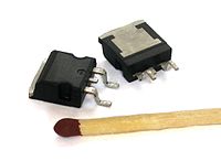
Photo from wikipedia
In spite of the reporting of several mathematical approaches dealing with the behavior of the superjunction MOSFET’s specific resistance, a study for the asymmetrical pillar (when the width of the… Click to show full abstract
In spite of the reporting of several mathematical approaches dealing with the behavior of the superjunction MOSFET’s specific resistance, a study for the asymmetrical pillar (when the width of the n-pillar and the p-pillar are not the same at a given cellpitch) has not been carried out yet. When the width of one of the pillar (say n-pillar) is modified, the doping concentration (say donor) should be changed to maintain a charge balance condition. This in turn, changes the width of the depletion region, due to the parasitic JFET effect and as a result the effective on-state conduction path. This raises the question whether the best tradeoff between the specific on-state resistance and the breakdown voltage could be achieved by employing the conventional assumption of the same width of the n and p pillars. This paper clarifies the best option for the width of each pillar when designing a superjunction MOSFET and adapts the figures of merit to take into account the asymmetrical superjunction cell.
Journal Title: IEEE Transactions on Electron Devices
Year Published: 2018
Link to full text (if available)
Share on Social Media: Sign Up to like & get
recommendations!