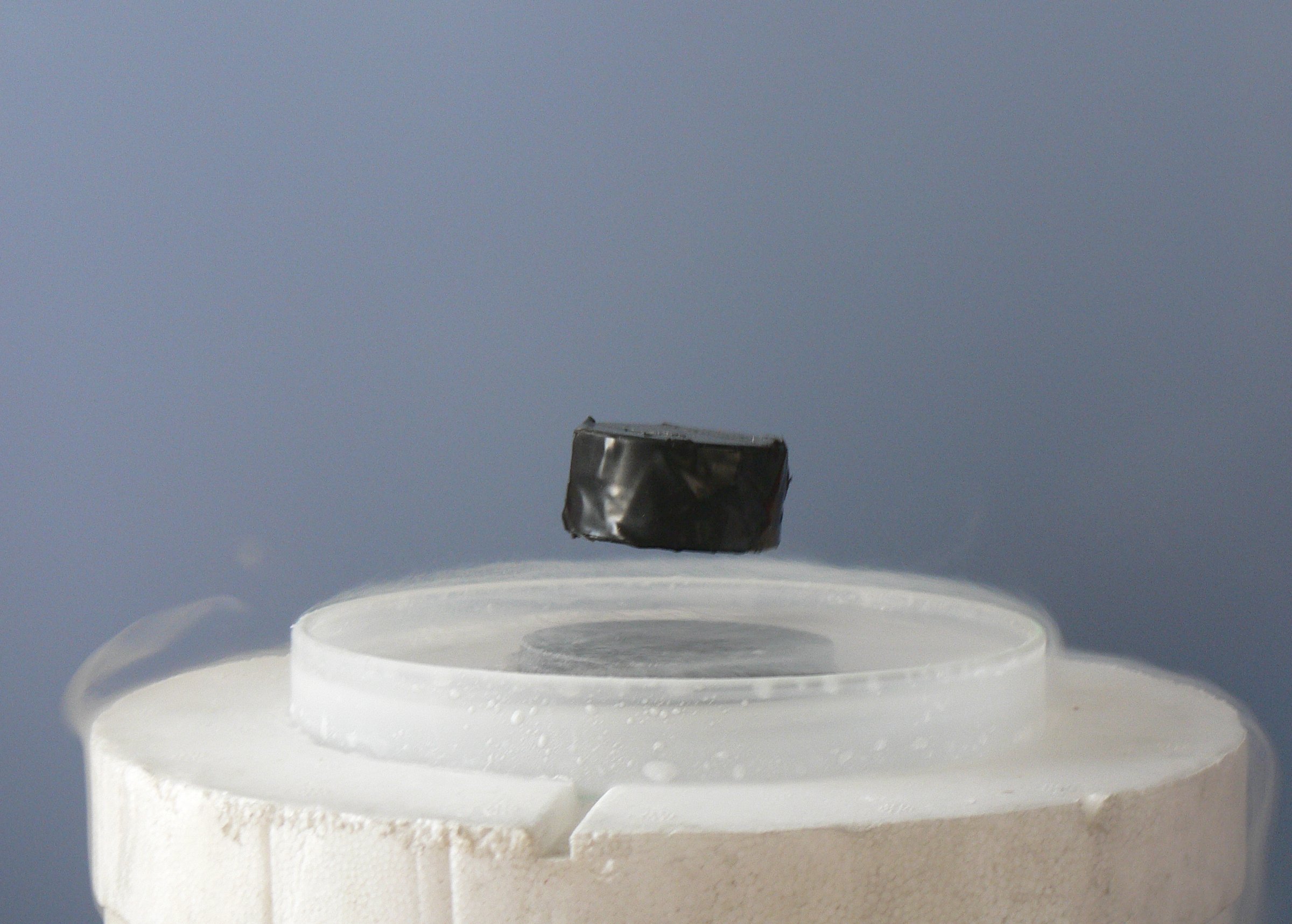
Photo from academic.microsoft.com
Three-dimensional structure and growth can be more appropriately realized through a nanomanufacturing process that uses a mask patterning and etching process. Unlike conventional single-wavelength ... Click to show full abstract
Three-dimensional structure and growth can be more appropriately realized through a nanomanufacturing process that uses a mask patterning and etching process. Unlike conventional single-wavelength ...
Journal Title: NANO
Year Published: 2019
Link to full text (if available)
Share on Social Media: Sign Up to like & get
recommendations!