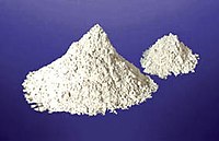
Photo from wikipedia
Atomic layers of hexagonal boron nitride (h-BN) crystal, primarily serving as atomically-smooth dielectric layers in two-dimensional (2D) electronics and structural materials in 2D nanoelectromechanical systems (NEMS), have recently emerged as… Click to show full abstract
Atomic layers of hexagonal boron nitride (h-BN) crystal, primarily serving as atomically-smooth dielectric layers in two-dimensional (2D) electronics and structural materials in 2D nanoelectromechanical systems (NEMS), have recently emerged as a promising platform for nanoscale optics and photonics. Ultrawide bandgap (~5.9 eV) of h-BN promises ultraviolet (UV) and deep ultraviolet (DUV) responsivity; it can host defect states related to single photon generation. Meanwhile, it also gives rise to the visibility challenge of these atomically-thin crystals, because of the optical transparency in the visible range. In this work, we conduct a comprehensive study, synergizing numerical modeling and experimental efforts, to reveal the optical contrast signatures of h-BN on various substrates. We demonstrate that the visualization and thickness identification based on optical contrast are applicable to mechanically suspended h-BN crystals, without interference enhancement from the commonly used oxidized silicon (SiO2 on Si) wafer. The understanding and protocols developed here offer a non-contact, rapid thickness estimation method for h-BN thin films on suspended device platforms, where conventional contact methods such as scanning probes are incapable or cumbersome. The results and methods presented here also serve as valuable guidelines for engineering the h-BN platform towards 2D nanophotonic and optoelectronic applications.
Journal Title: Optical Materials Express
Year Published: 2019
Link to full text (if available)
Share on Social Media: Sign Up to like & get
recommendations!