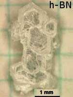
Photo from wikipedia
Defects and in-plane strain have significant effects on the electronic properties of two-dimensional nanostructures. However, due to the influence of substrate and environmental conditions, defects and strain are inevitable during… Click to show full abstract
Defects and in-plane strain have significant effects on the electronic properties of two-dimensional nanostructures. However, due to the influence of substrate and environmental conditions, defects and strain are inevitable during the growth or processing. In this study, hybrid density functional theory was employed to systematically investigate the electronic properties of boron-phosphide monolayers tuned by the in-plane biaxial strain and defects. Four types of defects were considered: B-vacancy (B_v), P-vacancy (P_v), double vacancy (D_v), and Stone–Wales (S-W). Charge density difference and Bader charge analysis were performed to characterize the structural properties of defective monolayers. All of these defects could result in the boron-phosphide monolayer being much softer with anisotropic in-plane Young’s modulus, which is different from the isotropic modulus of the pure layer. The calculated electronic structures show that the P_v, D_v, and S-W defective monolayers are indirect band gap semiconductors, while the B_v defective system is metallic, which is different from the direct band gap of the pure boron-phosphide monolayer. In addition, the in-plane biaxial strain can monotonically tune the band gap of the boron-phosphide monolayer. The band gap increases with the increasing tension strain, while it decreases as the compression strain increases. Our results suggest that the defects and in-plane strain are effective for tuning the electronic properties of the boron-phosphide monolayer, which could motivate further studies to exploit the promising application in electronics and optoelectronics based on the boron-phosphide monolayer.
Journal Title: Nanomaterials
Year Published: 2021
Link to full text (if available)
Share on Social Media: Sign Up to like & get
recommendations!