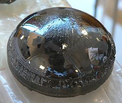
Finding unstrained 10 -nm lattice defects in silicon, given 1011 per cubic centimeter
Sign Up to like & getrecommendations! Published in 2017 at "Microscopy and Microanalysis"
DOI: 10.1017/s1431927617008157
Abstract: Our ability to image individual atoms and atom-columns only brings the practical problem of finding a statistically-useful number of nanoscale structures into sharper focus. In crystalline materials like metals and semiconductors, a key tool for… read more here.
Keywords: silicon given; lattice defects; unstrained lattice; defects silicon ... See more keywords

Computationally Driven Discovery of T Center-like Quantum Defects in Silicon.
Sign Up to like & getrecommendations! Published in 2024 at "Journal of the American Chemical Society"
DOI: 10.1021/jacs.4c06613
Abstract: Quantum technologies would benefit from the development of high-performance quantum defects acting as single-photon emitters or spin-photon interfaces. Finding such a quantum defect in silicon is especially appealing in view of its favorable spin bath… read more here.
Keywords: center like; quantum defects; quantum; center ... See more keywords

Magnetic-field-dependent spin properties of divacancy defects in silicon carbide.
Sign Up to like & getrecommendations! Published in 2023 at "Nanoscale"
DOI: 10.1039/d2nr06624f
Abstract: In recent years, spin defects in silicon carbide have become promising platforms for quantum sensing, quantum information processing and quantum networks. It has been shown that their spin coherence times can be dramatically extended with… read more here.
Keywords: coherence; defects silicon; spin properties; magnetic field ... See more keywords

Characterisation of crystalline defects in 4H Silicon Carbide using DLTS and TSC
Sign Up to like & getrecommendations! Published in 2025 at "Journal of Instrumentation"
DOI: 10.1088/1748-0221/20/07/c07006
Abstract: Future hadron collider experiments will require sensing materials that withstand stronger radiation fields. Therefore, either a frequent replacement of detectors, a significant increase in radiation hardness of Silicon, or a shift to different materials is… read more here.
Keywords: carbide; silicon carbide; crystalline defects; characterisation crystalline ... See more keywords

A method for alleviating the effect of pinhole defects from silicon nitride film in n-type rear-junction PERT silicon solar cells
Sign Up to like & getrecommendations! Published in 2023 at "Advances in Natural Sciences: Nanoscience and Nanotechnology"
DOI: 10.1088/2043-6262/acd241
Abstract: We investigated incorporation of a novel approach of phosphorous silicate glass layer thinning (PGT) process in the N-PERT process flow to minimise pinhole defects at the silicon nitride (Si3N4) surface. The thinning (PGT) process for… read more here.
Keywords: silicon nitride; pert; pinhole defects; pgt process ... See more keywords

Defects in Silicon Carbide as Quantum Qubits: Recent Advances in Defect Engineering
Sign Up to like & getrecommendations! Published in 2025 at "Applied Sciences"
DOI: 10.3390/app15105606
Abstract: This review provides an overview of defects in silicon carbide (SiC) with potential applications as quantum qubits. It begins with a brief introduction to quantum qubits and existing qubit platforms, outlining the essential criteria a… read more here.
Keywords: quantum qubits; carbide quantum; qubits recent; silicon carbide ... See more keywords

Electrically Active Defects in 3C, 4H, and 6H Silicon Carbide Polytypes: A Review
Sign Up to like & getrecommendations! Published in 2025 at "Crystals"
DOI: 10.3390/cryst15030255
Abstract: This paper aims to critically review electrically active defects studied by junction spectroscopy techniques (deep-level transient spectroscopy and minority carrier transient spectroscopy) in the three most commonly used silicon carbide (SiC) polytypes: 3C-SiC, 4H-SiC, and… read more here.
Keywords: spectroscopy; active defects; electrically active; silicon carbide ... See more keywords