
The influence of 2D MoS2 layers on the growth of GaN films by plasma-assisted molecular beam epitaxy
Sign Up to like & getrecommendations! Published in 2019 at "Applied Surface Science"
DOI: 10.1016/j.apsusc.2019.143616
Abstract: Abstract In the report, the growth of GaN films on the two-dimension molybdenum disulfide (2D MoS2) and c-sapphire via plasma-assisted molecular beam epitaxy (MBE) was investigated. Two kinds of MoS2 layers were prepared by pulsed… read more here.
Keywords: growth gan; mos2 layers; growth; surface ... See more keywords

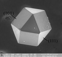
Effects of Al additives on growth of GaN polycrystals by the Na flux method
Sign Up to like & getrecommendations! Published in 2017 at "Optical Materials"
DOI: 10.1016/j.optmat.2016.09.030
Abstract: Abstract In this study, we investigated the growth of GaN polycrystals using the Al-added Na flux method. We studied the effects of Al on accelerating the nucleation and purity of GaN polycrystals. The yields of… read more here.
Keywords: added flux; gan polycrystals; growth gan; flux method ... See more keywords

Molecular beam epitaxy growth of GaN films on a tungsten carbide/Si template
Sign Up to like & getrecommendations! Published in 2018 at "Thin Solid Films"
DOI: 10.1016/j.tsf.2018.01.057
Abstract: Abstract This study examined the growth of GaN layers by molecular beam epitaxy (MBE) using a tungsten carbide (WC) buffer sputtered on a Si(111) surface. The chemical stability of the WC layer against the Ga-Si… read more here.
Keywords: growth gan; molecular beam; beam epitaxy; growth ... See more keywords
Size control of GaN nanocrystals formed by ion implantation in thermally grown silicon dioxide
Sign Up to like & getrecommendations! Published in 2020 at "Journal of Applied Physics"
DOI: 10.1063/1.5132604
Abstract: The growth of GaN nanocrystals in an amorphous SiO2 matrix by sequential Ga and N implantation and rapid thermal annealing is reported. The effect of the implantation and annealing conditions on the distribution of the… read more here.
Keywords: microscopy; implantation annealing; growth gan; size ... See more keywords

Numerical Simulation of Ammonothermal Crystal Growth of GaN—Current State, Challenges, and Prospects
Sign Up to like & getrecommendations! Published in 2021 at "Crystals"
DOI: 10.3390/cryst11040356
Abstract: Numerical simulations are a valuable tool for the design and optimization of crystal growth processes because experimental investigations are expensive and access to internal parameters is limited. These technical limitations are particularly large for ammonothermal… read more here.
Keywords: growth gan; ammonothermal growth; crystal growth; growth ... See more keywords

MOVPE Growth of GaN via Graphene Layers on GaN/Sapphire Templates
Sign Up to like & getrecommendations! Published in 2022 at "Nanomaterials"
DOI: 10.3390/nano12050785
Abstract: The remote epitaxy of GaN epilayers on GaN/sapphire templates was studied by using different graphene interlayer types. Monolayer, bilayer, double-stack of monolayer, and triple-stack of monolayer graphenes were transferred onto GaN/sapphire templates using a wet… read more here.
Keywords: graphene; microscopy; growth gan; gan sapphire ... See more keywords

In(Ga)N 3D Growth on GaN-Buffered On-Axis and Off-Axis (0001) Sapphire Substrates by MOCVD
Sign Up to like & getrecommendations! Published in 2022 at "Nanomaterials"
DOI: 10.3390/nano12193496
Abstract: In(Ga)N epitaxial layers were grown on on-axis and off-axis (0001) sapphire substrates with an about 1100 nm-thick GaN buffer layer stack using organometallic chemical vapor deposition at 600 °C. The In(Ga)N layers consisted of a… read more here.
Keywords: axis axis; 0001 sapphire; sapphire substrates; growth gan ... See more keywords