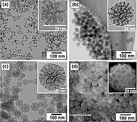
Wet-Chemical Etching: a Novel Nanofabrication Route to Prepare Broadband Random Plasmonic Metasurfaces
Sign Up to like & getrecommendations! Published in 2019 at "Plasmonics"
DOI: 10.1007/s11468-018-0813-4
Abstract: Broadband optical metasurfaces are gaining enormous attention owing to their potential applications in optoelectronic devices, sensors, and flat optics. Here, we demonstrate for the first time a single-step, novel wet-chemical etching-based nanofabrication method to produce… read more here.
Keywords: broadband; random plasmonic; nanofabrication; wet chemical ... See more keywords

Large-Scale Nanofabrication of Designed Nanostructures Using Angled Nanospherical-Lens Lithography for Surface Enhanced Infrared Absorption Spectroscopy.
Sign Up to like & getrecommendations! Published in 2017 at "ACS applied materials & interfaces"
DOI: 10.1021/acsami.7b08994
Abstract: Nanophotonics has been a focused research discipline for the past decade and has resulted in many novel concepts that promise to change human life. However, the actual penetration of this research into real products is… read more here.
Keywords: large scale; angled nanospherical; nanospherical lens; spectroscopy ... See more keywords

Three-dimensional nanofabrication via ultrafast laser patterning and kinetically regulated material assembly
Sign Up to like & getrecommendations! Published in 2022 at "Science"
DOI: 10.1126/science.abm8420
Abstract: A major challenge in nanotechnology is the fabrication of complex three-dimensional (3D) structures with desired materials. We present a strategy for fabricating arbitrary 3D nanostructures with a library of materials including metals, metal alloys, 2D… read more here.
Keywords: wide range; femtosecond light; three dimensional; assembly ... See more keywords

Scanning Probe Lithography: State-of-the-Art and Future Perspectives
Sign Up to like & getrecommendations! Published in 2022 at "Micromachines"
DOI: 10.3390/mi13020228
Abstract: High-throughput and high-accuracy nanofabrication methods are required for the ever-increasing demand for nanoelectronics, high-density data storage devices, nanophotonics, quantum computing, molecular circuitry, and scaffolds in bioengineering used for cell proliferation applications. The scanning probe lithography… read more here.
Keywords: scanning probe; nanofabrication; probe lithography; state art ... See more keywords

Versatile Approach of Silicon Nanofabrication without Resists: Helium Ion-Bombardment Enhanced Etching
Sign Up to like & getrecommendations! Published in 2022 at "Nanomaterials"
DOI: 10.3390/nano12193269
Abstract: Herein, we report a helium ion-bombardment enhanced etching method for silicon nanofabrication without the use of resists; furthermore, we demonstrate its unique advantages for straightforward fabrication on irregular surfaces and prototyping nano-electro-mechanical system devices, such… read more here.
Keywords: bombardment enhanced; ion bombardment; nanofabrication; silicon ... See more keywords