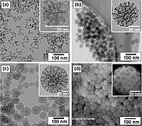
Core-Shell C@Sb Nanoparticles as a Nucleation Layer for High-Performance Sodium Metal Anodes.
Sign Up to like & getrecommendations! Published in 2020 at "Nano letters"
DOI: 10.1021/acs.nanolett.0c01257
Abstract: Sodium metal anode (SMA) is one of the most favored choices for the next-generation rechargeable battery technologies owing to low cost and natural abundance. However, the poor reversibility resulted from dendrite growth and formation of… read more here.
Keywords: nucleation layer; core shell; shell nanoparticles; sodium ... See more keywords

Titanium Carbide MXene Nucleation Layer for Epitaxial Growth of High-Quality GaN Nanowires on Amorphous Substrates.
Sign Up to like & getrecommendations! Published in 2020 at "ACS nano"
DOI: 10.1021/acsnano.9b09126
Abstract: Growing III-nitride nanowires on 2D materials is advantageous as it effectively decouples the underlying growth substrate from the properties of the nanowires. As a relatively new family of 2D materials, MXenes are promising candidates as… read more here.
Keywords: quality; epitaxial growth; nucleation layer; gan nanowires ... See more keywords

Toward efficient long-wavelength III-nitride emitters using a hybrid nucleation layer.
Sign Up to like & getrecommendations! Published in 2021 at "Optics express"
DOI: 10.1364/oe.430721
Abstract: The realization of efficient III-nitride emitters in the green-to-amber region is fundamental to the monolithic integration of multicolor emitters and the development of III-nitride-based full-color high-resolution displays. A hybrid nucleation layer, which includes sputtered AlN… read more here.
Keywords: iii nitride; nucleation layer; nucleation; nitride emitters ... See more keywords

The Effect of a Nucleation Layer on Morphology and Grain Size in MOCVD-Grown β-Ga2O3 Thin Films on C-Plane Sapphire
Sign Up to like & getrecommendations! Published in 2022 at "Materials"
DOI: 10.3390/ma15238362
Abstract: β-Ga2O3 thin films grown on widely available c-plane sapphire substrates typically exhibit structural defects due to significant lattice and thermal expansion mismatch, which hinder the use of such films in electronic devices. In this work,… read more here.
Keywords: nucleation; plane sapphire; nucleation layer; ga2o3 thin ... See more keywords