
Light Emission of Self‐Trapped Excitons in Inorganic Metal Halides for Optoelectronic Applications
Sign Up to like & getrecommendations! Published in 2022 at "Advanced Materials"
DOI: 10.1002/adma.202201008
Abstract: Self‐trapped excitons (STEs) have recently attracted tremendous interest due to their broadband emission, high photoluminescence quantum yield, and self‐absorption‐free properties, which enable a large range of optoelectronic applications such as lighting, displays, radiation detection, and… read more here.
Keywords: trapped excitons; self trapped; optoelectronic applications; emission ... See more keywords
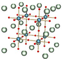
Screen printing coating of (ZnO)0.8(CdO)0.2 material for optoelectronic applications
Sign Up to like & getrecommendations! Published in 2020 at "Optical and Quantum Electronics"
DOI: 10.1007/s11082-020-02511-5
Abstract: Here we report X-ray response and optical properties of composite (ZnO)0.8(CdO)0.2 thick film deposited by simple, easy and low cost screen printing technique on glass substrates followed by sintering at 500 °C. X-ray diffraction pattern confirms… read more here.
Keywords: optoelectronic applications; screen printing; coating zno; zno cdo ... See more keywords

A solution-processed nanoscale COF-like material towards optoelectronic applications
Sign Up to like & getrecommendations! Published in 2020 at "Science China Chemistry"
DOI: 10.1007/s11426-020-9865-3
Abstract: Two-dimensional (2D) covalent organic frameworks (COFs) with periodic functional n-electron systems are an emerging class of optoelectronic materials. However, almost all conjugated COFs so far are insoluble and hard to process, which hampers severely their… read more here.
Keywords: pdpp c20; optoelectronic applications; like material; cof like ... See more keywords

Fabrication of plasmonic gold-nanoparticle-transition metal oxides thin films for optoelectronic applications
Sign Up to like & getrecommendations! Published in 2019 at "Journal of Alloys and Compounds"
DOI: 10.1016/j.jallcom.2018.10.055
Abstract: Abstract A simple, cost-effective, and one-step procedure for fabrication of gold-nanoparticle-transition metal oxide (Au-TMO) thin films with tuned optical and structural properties is described. In this approach, a homogeneous mixed precursor solution was used to… read more here.
Keywords: transition metal; fabrication; thin films; optoelectronic applications ... See more keywords

The spintronic and optoelectronic applications of substitutional doped CoS2
Sign Up to like & getrecommendations! Published in 2021 at "Materials Chemistry and Physics"
DOI: 10.1016/j.matchemphys.2021.125052
Abstract: Abstract The structural, electronic, magnetic and optical properties of the substitutional doped CoS2 by B, C, Si and Al atoms have been investigated by first–principles method, considering four doping concentration. The heavy doped CoX0.50S1.50, CoX0.25S1.75… read more here.
Keywords: substitutional doped; doped cos2; spintronic optoelectronic; applications substitutional ... See more keywords

Two step vapor-processing and experimental investigations of all-inorganic CsPbCl3 perovskite films for optoelectronic applications
Sign Up to like & getrecommendations! Published in 2021 at "Materials Letters"
DOI: 10.1016/j.matlet.2021.129819
Abstract: Abstract Inorganic perovskites (CsPbX3, X= I-, Br-or Cl-) have got researchers attention in the photovoltaic community due to their exceptional photoelectric properties and high thermal stability. In this work, we have explained a two-step vapor… read more here.
Keywords: two step; cspbcl3 perovskite; perovskite films; step vapor ... See more keywords
Advances in metal halide perovskite nanocrystals: Synthetic strategies, growth mechanisms, and optoelectronic applications
Sign Up to like & getrecommendations! Published in 2020 at "Materials Today"
DOI: 10.1016/j.mattod.2019.06.007
Abstract: Abstract Metal halide perovskite nanocrystals, as a new class of light-harvesting and light-emitting materials, have recently attracted a lot of attention for an impressive variety of optoelectronic applications. Some advantages of perovskite nanocrystals include there… read more here.
Keywords: halide perovskite; metal halide; growth mechanisms; perovskite nanocrystals ... See more keywords

Bulky Organic Cations Engineered Lead-halide Perovskites: A Review on Dimensionality and Optoelectronic Applications
Sign Up to like & getrecommendations! Published in 2021 at "Materials Today Energy"
DOI: 10.1016/j.mtener.2021.100759
Abstract: Abstract Hybrid lead-halide perovskites are widely used in a variety of optoelectronic applications, including perovskite solar cells (PSCs), perovskite light-emitting diodes (PeLEDs), perovskite photodetectors (PPDs), and scintillators. Recently, it was demonstrated that bulky organic cations… read more here.
Keywords: halide perovskites; lead halide; bulky organic; organic cations ... See more keywords

Cu sputtered Cu/ZnO Schottky diodes on fluorine doped tin oxide substrate for optoelectronic applications
Sign Up to like & getrecommendations! Published in 2019 at "Thin Solid Films"
DOI: 10.1016/j.tsf.2019.04.019
Abstract: Abstract In the present work, ZnO thin films were deposited on fluorine doped tin oxide (FTO) and soda lime glass substrates using sol-gel spin coating technique. Cu thin films were deposited on ZnO by the… read more here.
Keywords: zno schottky; thin films; fluorine doped; doped tin ... See more keywords

Self-Assembly and Regrowth of Metal Halide Perovskite Nanocrystals for Optoelectronic Applications
Sign Up to like & getrecommendations! Published in 2022 at "Accounts of Chemical Research"
DOI: 10.1021/acs.accounts.1c00651
Abstract: Conspectus Over the past decade, the impressive development of metal halide perovskites (MHPs) has made them leading candidates for applications in photovoltaics (PVs), X-ray scintillators, and light-emitting diodes (LEDs). Constructing MHP nanocrystals (NCs) with promising… read more here.
Keywords: self assembly; optoelectronic applications; metal halide; assembly regrowth ... See more keywords

van der Waals Epitaxy of Organic Semiconductor Thin Films on Atomically Thin Graphene Templates for Optoelectronic Applications.
Sign Up to like & getrecommendations! Published in 2022 at "Accounts of chemical research"
DOI: 10.1021/acs.accounts.1c00686
Abstract: ConspectusOrganic semiconductors (OSCs) offer unique advantages with respect to mechanical flexibility, low-cost processing, and tunable properties. The optical and electrical properties of devices based on OSCs can be greatly improved when an OSC is coupled… read more here.
Keywords: graphene; van der; growth; optoelectronic applications ... See more keywords